Double data rate

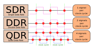
In computing, a computer bus operating with double data rate (DDR) transfers data on both the rising and falling edges of the clock signal.[1] This is also known as double pumped, dual-pumped, and double transition. The term toggle mode is used in the context of NAND flash memory.
The simplest way to design a clocked electronic circuit is to make it perform one transfer per full cycle (rise and fall) of a clock signal. This, however, requires that the clock signal changes twice per transfer, while the data lines change at most once per transfer. When operating at a high bandwidth, signal integrity limitations constrain the clock frequency. By using both edges of the clock, the data signals operate with the same limiting frequency, thereby doubling the data transmission rate.
This technique has been used for microprocessor front side busses, Ultra-3 SCSI, graphics RAM (the AGP bus and GDDR), main memory (both RDRAM and DDR1 through DDR4), and the HyperTransport bus on AMD's Athlon 64 processors. It is more recently being used for other systems with high data transfer speed requirements – as an example, for the output of analog-to-digital converters (ADCs).[2]
DDR should not be confused with dual channel, in which each memory channel accesses two RAM modules simultaneously. The two technologies are independent of each other and many motherboards use both, by using DDR memory in a dual channel configuration.
An alternative to double or quad pumping is to make the link self-clocking. This tactic was chosen by InfiniBand and PCI Express.
Relation of bandwidth and frequency
Describing the bandwidth of a double-pumped bus can be confusing. Each clock edge is referred to as a beat, with two beats (one upbeat and one downbeat) per cycle. Technically, the hertz is a unit of cycles per second, but many people refer to the number of transfers per second. Careful usage generally talks about "500 MHz, double data rate" or "1000 MT/s", but many refer casually to a "1000 MHz bus," even though no signal cycles faster than 500 MHz.
DDR SDRAM popularized the technique of referring to the bus bandwidth in megabytes per second, the product of the transfer rate and the bus width in bytes. DDR SDRAM operating with a 100 MHz clock is called DDR-200 (after its 200 MT/s data transfer rate), and a 64-bit (8-byte) wide DIMM operated at that data rate is called PC-1600, after its 1600 MB/s peak (theoretical) bandwidth. Likewise, 1.6 GT/s transfer rate DDR3-1600 is called PC3-12800.
Some examples of popular designations of DDR modules:
| Names | Memory clock | I/O bus clock | Transfer rate | Theoretical bandwidth |
|---|---|---|---|---|
| DDR-200, PC-1600 | 100 MHz | 100 MHz | 0.2 GT/s | 1.6 GB/s |
| DDR2-800, PC2-6400 | 200 MHz | 400 MHz | 0.8 GT/s | 6.4 GB/s |
| DDR3-1600, PC3-12800 | 200 MHz | 800 MHz | 1.6 GT/s | 12.8 GB/s |
| DDR4-3200, PC4-25600 | 400 MHz | 1600 MHz | 3.2 GT/s | 25.6 GB/s |
DDR SDRAM uses double-data-rate signalling only on the data lines. Address and control signals are still sent to the DRAM once per clock cycle (to be precise, on the rising edge of the clock), and timing parameters such as CAS latency are specified in clock cycles. Some less common DRAM interfaces, notably LPDDR2, GDDR5 and XDR DRAM, send commands and addresses using double data rate.
See also
- DDR SDRAM, DDR2 SDRAM, DDR3 SDRAM and DDR4 SDRAM (which all use DDR signalling)
- List of device bit rates
- Pumping (computer systems)
- Quad data rate
References
- ↑ Hennessy, John L.; Patterson, David A.; Arpaci-Dusseau, Andrea.; … (2007). Computer architecture : a quantitative approach. Amsterdam: Morgan Kaufmann. ISBN 0-12-370490-1.
- ↑ "AD9467 ADC" (PDF) (data sheet). Analog Devices.